PCB cloning is the process of building a replica of a Printed circuit board by extracting information from it. It involves copying features and specifications of an already existing PCB.
The result of cloning PCB is known as a PCB clone and is used by electronic manufacturers to produce products in a cost-efficient and quick manner.
A PCB clone is made up by the process of reverse engineering, It includes the use of software and hardware tools along with professional expertise.
It is becoming increasingly popular and widely accepted in the PCB industry as it saves time, money, and resources.
Stick till the end to learn more about PCBs and learn how PCB clones are made. Also, learn about How Artificial Intelligence is Shaping Our World by reading this article.
PCB cloning is done for a variety of reasons. Some of the reasons are as follows
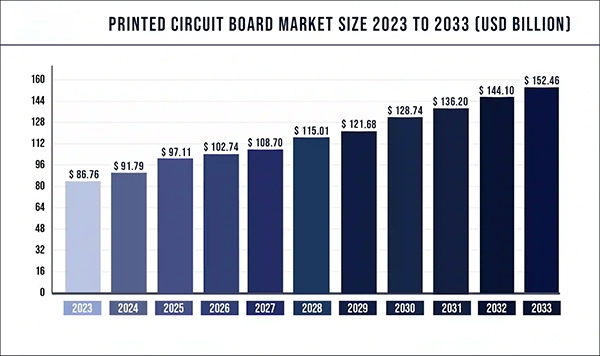
Due to the numerous benefits and uses of PCB, It can be estimated it is a growing market The following graph depicts the rise in the market size of printed circuit boards
Traditionally, PCB cloning was considered a complex process but with the help of reverse engineering, it has simplified a lot. PCB cloning can be done in the following steps-
Carefully examine the printed circuit board that needs to be copied. You can even click pictures to help you out later in the process.
Desolder all the components from the circuit and clean the circuit using alcohol to clean any remnants left.
Scan the circuit at a high resolution to obtain clear images of the board. Polish the top and bottom layers using sandpaper to reveal the copper traces and repeat the process of imaging.
Check the images for any imperfections or inconsistencies, you can use any editing software to rectify it.
Import the top and bottom layer images into a designing software. Overlay the images, if they align perfectly it means that the imaging was done correctly.
If they do not align, it signals a fault in the previous step and requires it to be done again. Start tracing the copper traces in the design software carefully. Trace all the layers until the whole design is completely traced.
Once the layout is done, you can export the BOM as Gerber files and send it to a fabrication house to produce that replica.
Once the board is fabricated, you can place all the components on the board as examined initially. You can refer to the images taken in step one to recreate the PCB.
When the assembling is done, you can test the functionality and performance of the board and compare the replica to the original PCB board.
PCB cloning is subject to the same rules and regulations as the original one. It is essential to abide by all the laws while cloning a PCB.
There are some important aspects to bear in mind during the process such as copyright infringement, patent, trademark infringement, and trade secret law.
Cloning a PCB involves various intricate steps. Even a small slip can result in undesired results and wreck the whole process. Stay focused while scanning, imaging, tracing, and reassembling the board. All the components need to be accurately traced and placed to get the desired result.
The time and cost to clone a PCB vary according to the components and techniques used. It proves to be a cost-effective and time-saving technique as it saves from the hassle of building PCB boards from scratch.
To make a PCB clone work properly, it is mandatory to use compatible components. While making a PCB consider how the components interact together in the external system.
TRIVIAMost PCBs are green due to the reflection of their solder masks that show through the epoxy. They can show a variation of color and come in orange, blue, or yellow colors.
PCB cloning has proved to be a game changer for companies that work with multiple variations of the same printed circuit boards
It is used in numerous electronic devices including medical, security, industrial, and maritime equipment. From toy cars to huge automobiles, it is used everywhere.
It can be gathered that the demands for PCB are high and it is likely to increase even more in the future and so will the demand for PCB cloning.
.

Thanks for choosing to leave a comment. Please keep in mind that all comments are moderated according to our comment Policy.